Published
by Guillem Gargallo, Market Development Manager
Advanced Electronics Solutions
When using SiC, a key aspect to consider is how to dissipate the losses from a smaller area compared to that of Si devices. The higher cost of these devices is pushing many to reduce the die size to a minimum, further enhancing the challenge of dissipating the losses without increasing the total system costs.
Multiple recent power module concepts have been released to address this challenge; one thing most of them have in common is their utilization of metallized ceramic substrates. Their superior mechanical, thermal and electrical characteristics make them an essential element in the design of power modules for EV traction applications. It is important to pay special attention when selecting the substrate's material combination to achieve the best thermal performance, meet reliability requirements and optimize costs.
The questions arise — what is the best material combination, and should an HPS (Zr doped Al2O3) substrate with 0.3 mm Cu be selected? On the one hand, there can be good mechanical stability at a great cost, yet have limited thermal performance. Or, what if the Cu thickness is increased to 0.6 mm? Also, what if the substrate is changed to Si3N4, increasing the cost but also the thermal performance?
There are no simple answers to the "what if" questions.
To help customers answer these questions and accelerate their decisions, the team at Rogers developed a series of simulation tools using our extensive experience. In this blog, we will showcase a small portion of these simulation tools using a simplified thermal model. This simulation could be extended to include customized layouts, different module constructions (e.g., baseplate with or without fins; dual-side cooling; etc.) or other material combinations to analyze impacts on a specific design in more detail. Additionally, it is possible to run a more in-depth fluid analysis using the FEM simulation, as well as lifetime prediction models.
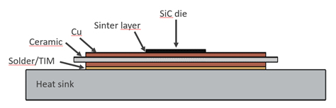
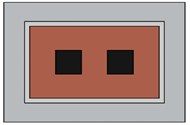
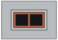
To keep things simple for the purpose of this blog, we used a basic generic model, based on a classic baseless module connected to a copper water cooler at a constant temperature (see Figure 1). The module is either soldered to the heat sink or connected to a thermal interface material (TIM). We compared substrate materials and Cu thicknesses (see Table 1) on two different layouts. The first layout has enough Cu area around the dice to enable a good thermal spreading (see Figure 2). On the second layout, the dice is as close as possible and has a minimal Cu area around them (see Figure 3). In order to further simplify the model, we considered a single heat transfer coefficient of 15000 W/m2K for the heat sink and a constant loss of 200 W per die.
The model could be made significantly more complex. Customized layouts, dynamic losses, specific heat sink profiles or interconnection technologies are among the parameters that could be adapted to a specific request.
Figure 1: cross-section simplified model
| Layer | Material (Thermal conductivity [W/mK]) | Layer thickness [mm] |
| Chip | SiC (370) | 0,2 |
| Sinter layer | Sinter-Ag (250) | 0,05 |
| Top Cu | Cu (395) | 0,2 - 2,0 |
| Ceramic | HPS (26) / Si3N4 (90) / HC Si3N4 (120) /AlN (180) | 0,25/0,32/0,38/0,63 |
| Bottom Cu | Cu (395) | 0,2 - 2,0 |
| Solder/TIM | SAC (50) /TIM (3,4) | 0,2/0,1 |
| Heat sink | Cu (395) | 2 |
Figure 2: Layout 1; 5x5mm SiC dice with 5mm free Cu around them
Figure 3: Layout 2; 5x5 SiC dice with 1mm free Cu around them
Table 1: Materials and properties used for the simulation
With the model built, we can look at several possible scenarios. We could analyze several different influencing parameters, such as the ceramic material, its thickness, the Cu thickness, the influence of the interconnection to the heat sink (TIM or solder/sinter), the distance between chips and many more. In order to keep it simple, we concentrated on just a couple of scenarios, but nevertheless a more in-depth analysis could be conducted upon request.
We know that some of the temperatures presented in the figures below are well beyond any design targets. They are not meant to be take literally, but rather as an indication to compare different solutions. Another approach to this would have been to normalize the results.
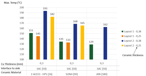
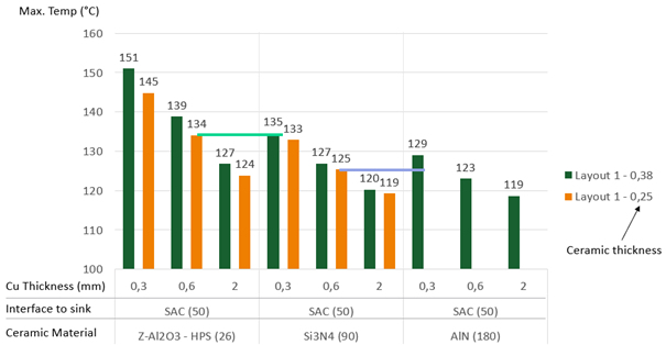
In a first stage we will compare the influence of the ceramic substrate material with the two different layouts on the chip temperature. In Figure 4, the comparison can be observed when using either a solder material to the heat sink or a standard 0.3 mm Cu thickness for all solutions.
Figure 4: Maximum chip temperature for different ceramic materials and thicknesses with 0.3mm Cu and soldered to the heat sink with a SAC material
The graphic above contains a lot of information, but firstly, we can highlight the significant difference between Layout 1 and 2 regardless of the material combination. This highlights the need to have sufficient Cu area around the dice to facilitate the heat spreading. The influence of the layout could be reduced with a higher heat transfer coefficient to the ambient that would enhance the thermal dissipation in the y-axis. Nevertheless, sufficient Cu area around the dice should be used, if possible.
As expected, using ceramic materials with a higher thermal conductivity result in a lower temperature. For the same material thickness, there is a big step between HPS and the remaining materials. However, the difference between a standard Si3N4 with 90 W/mK and AlN, which has doubled the thermal conductivity, is still visible but less pronounced.
We can also observe that material thickness can bring you an extra degree Celsius that it is needed to meet design parameters, which is especially true for HPS.
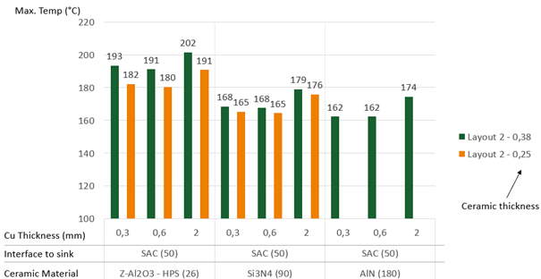
Unfortunately, an improvement on the ceramic substrate does not come for free and, in some designs, the increase in the ceramic's cost cannot be justified. A more economical alternative would be to increase the thickness of the Cu layer, e.g. from 0.3 to 0.6 or even 2 mm. The later brings some design and reliability challenges but it is still worth considering. The result of the comparison of the different Cu thicknesses can be seen in Figure 5 and 6 with layout 1 and 2 respectively.
Figure 5: Maximum chip temperature for different ceramic and Cu thicknesses, soldered to the heat sink with a SAC material. Only for Layout 1
In Figure 5, we can clearly observe that when enough Cu is around the dice, increasing the thickness of this layer can bring a tremendous benefit to the system. For instance, a 0.6mm Cu layer used with a 0.25 mm HPS can achieve a similar chip temperature as a 0.3 mm Cu Si3N4 at a better cost (green line). Moreover, a 0.6 mm Cu Si3N4 could also improve the performance compared to a 0.3 mm Cu AlN with a better reliability.
An even thicker Cu layer of 2mm brings yet an additional improvement in the chip temperature. At this point, we can see a certain saturation in the improvement, and thicker Cu would not bring any significant benefit.
Of course, it is not always possible to place the dice with enough Cu area around it. In case the layout is more compact, the situation changes completely as can be observed in Figure 6.
Figure 6: Maximum chip temperature for different ceramic and Cu thicknesses, soldered to the heat sink with a SAC material. Only for Layout 2
In this case the thicker Cu does not bring any added value, as the dice does not benefit from the spreading effect of the thicker Cu. Moreover, for very thick Cu layers, such as 2mm, the added material hinders the thermal conduction in the y-axis, reducing the Rth and thus increasing the chip temperature. Overall, thicker Cu might be an advantage under certain conditions, but it is not always the best solution.
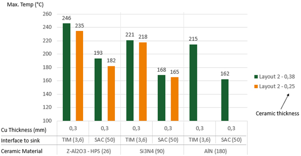
So far, we have focused on the substrates. There are of course many other barriers in the thermal path, with the interface to the heat sink being one of the most relevant. In Figure 7 we can see the results of this comparison.
Figure 7: Maximum chip temperature for different ceramics, soldered to the heat sink with a SAC material or connected with a standard TIM. Only for Layout 2
Regardless of which ceramic substrate is used, the temperature differences are quite striking. The temperatures are in both cases out of most design targets; nevertheless, it shows the relevance of this interface layer in the overall design. One could argue that the thickness for the TIM layer (100 µm) and the material itself could be further optimized, but so could the solder material.
Deciding on the best set of materials for your power module can be a laborious task. Many different parameters must be considered to find the best solution, such as the ceramic material, its thickness, the thickness of the Cu, the interface to the heat sink, the cooling method and so on. Doing this by trial-and-error testing is impractical, and the support of simulation tools is necessary to ensure adequate time-to-market and development costs.
At Rogers we have developed a series of tools to help our customers and to support their decision making. In this blog we have showed a small part of these tools with a simple thermal model. Other aspects, such as reliability and cost, can also be simulated to complete the picture. Furthermore, the thermal model can be adapted to more complex and real environments. We are committed to extending and improving these tools and using them to the service of our customers to help reduce their design costs and to save time.
Do you have any questions or require more information about our ceramic substrates? Please contact us, if you need assistance.
Published on Apr 27, 2022