Published
by Olivier Mathieu, Market Development Manager
Advanced Electronics Solutions
The beginning of a new year is a time for resolutions. It is also a perfect opportunity to discuss key principles to design custom Direct Bonded Copper (DBC) and Active Metal Brazed (AMB) substrates. Design engineers should not be the only ones who know how to optimize their designs; process and quality engineers and their colleagues in procurement and purchasing should be aware of the various design options, their advantages and drawbacks. If you are a young engineer, let us share our knowledge! If you are an experienced engineer, let us refresh your knowledge!
Master card format
For many years, Rogers has been producing DBC and AMB substrates in master card format to accommodate multiple single units on one panel. The 7.5” x 5.5” master card has become a standard ceramic size with many suppliers delivering alumina (Al2O3), aluminum nitride (AlN) and silicon nitride (Si3N4) in this format. Production equipment and tools are designed to handle this format along the process chain, from incoming to final inspection. Then, copper sheets are stamped from the coil in a slightly smaller format and placed on the master card in a way which allows customers to use up to 7” x 5” of the original master card size for each single unit.
Various shapes and delivery options
DBC and AMB substrates can be produced in various shapes but the least expensive to produce is rectangular. Rectangular substrates can be easily arranged next to each other without any lateral gaps between units. A fast and easy-to-implement laser scribing process pre-cuts the substrates on their periphery to enable a manual or automated breaking along the scribing lines. Of course, a laser cutting process could be used instead of laser scribing; however, laser cutting is significantly slower than laser scribing. Once the substrates have been cut, the tools and equipment for the following processes, such as surface cleaning and plating, should be designed to handle multiple sizes of single units, instead of a unique master card size. This option is not commercially viable.
On request, chamfers can be accommodated on the corners of the substrates, 45° chamfers are common but other angles are possible too. As long as they do not vary in their angle and size, such chamfers can be produced without sacrificing any additional surface between each single unit. Additionally, chamfers should neither be too small nor too large when compared to the length and width of the substrate. Chamfers that are too large may cause undesired breakage during production as a result of insufficient stability of the master card, while chamfers that are too small can no longer be broken. Cutouts, notches and recesses can be implemented without any additional costs, but we strongly recommend that you let our Rogers Power Electronics Solutions (PES) team check your design before you spend money for any expensive tool for your module.
Round, ellipsoidal or other elaborate shapes are possible, though they require laser cutting to separate from the master card. Substrates are usually delivered as single units, but rectangular substrates can be delivered in master card format with or without pre-cutting. The option best fit for your company depends on your business model. Some module manufacturers need few substrates in large quantities while others require multiple substrates in small quantities. Delivery as single units or in master card format can make a difference depending on the kind of production equipment and tools that you are using or planning to use. Single units are easier to jump-start and hence the best way to get started on a new design. Depending, master card format can be the superior choice, if you want to streamline your equipment and tooling costs while optimizing your labor and process costs for large volume production.
Optimize substrate size to maximize master card surface area
Depending on the size and shape of your single units, you can accommodate one up to a thousand of substrates per master card. While very large and very small substrates are possible in theory, they come with their specific problems. Very small substrates require a long process time for laser scribing, breaking, final inspection and packaging. Special breaking tools and customized packaging trays are often necessary to satisfy and fulfill the product requirements. The experience has shown that substrates with a length and width less than 15 mm can be significantly more expensive to produce. On the contrary, very large substrates are easier to handle but can only be produced from the best quality substrates. Low quality substrates lead to multiple defects per substrate surface area, and are rejected during final inspection.
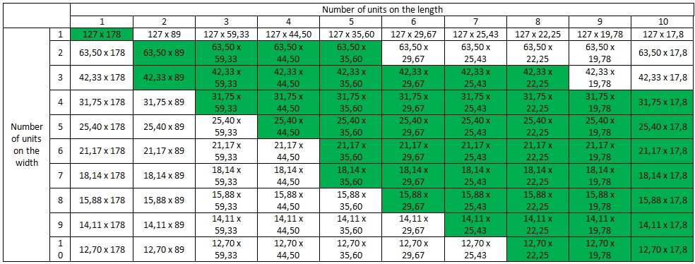
Another key consideration when designing your substrate is to fully maximize the available 7”x 5” master card surface. Any surface that is not used by your design will be scrapped while still contributing to the overall substrate cost. Ideally, your substrate size should be chosen to achieve 100% utilization illustrated below in Figure 1 for 1-100 rectangular substrates per master card. In theory, any kind of rectangular substrate is possible, but long stripes are less common than square substrates. Depending on the available footprint for substrates in your application, the length to width ratio should not exceed factor “2,” as this may lead to excessive bending of the single units. Bending is a critical parameter for the die assembly process and later for the assembly with base plate or heat sinks. Unfortunately, substrates are not perfectly flat and their bending can be influenced by multiple factors, such as shape, size, length to width ratio, arrangement along the long or short side of the master card, circuit layout, copper and ceramic thickness. Please refer to our technical notes and get in touch with our PES technical support team to learn more about flatness and bending of substrates.
Figure 1: substrate sizes for 100% utilization of the available master card surface
We hope that this was useful to help design your next DBC and AMB substrates. As a manufacturer of metallized ceramic substrates and with a full range of DBC and AMB substrates to address the needs from different markets, Rogers' PES team is available to help as your development partner.
Do you have any question or require some support with the design and selection of a suitable substrate for your application? Please contact us, if you need assistance. The information herein is for reference only. Neither the author nor Rogers makes any warranties as to its contents.
Related Products:
curamik Ceramic Substrates
Tags:
Aerospace & Defense, Automotive & EV/HEV, General Industrial, Major Appliances, Wind & Solar
Published on Jan 09, 2020